
































China produces 7-nanometer chips used in Huawei’s flagship smartphones and AI accelerators. It does this without a single ASML extreme ultraviolet (EUV) lithography machine — the $200-million-plus system that many engineers call the most complex machine ever built, and the one tool Western export controls are designed to deny it.
The common assumption is that without EUV, advanced chips are impossible. China has spent the last few years proving that assumption is only partially true.
This article explains exactly how — and, just as importantly, at what price. Because the real story is not that China found a magic workaround. It is that China accepted brutal economic penalties to build near-frontier chips with older tools, and then optimized everything else around that constraint.
In this article:
- What EUV actually is, and why it is called the most complex machine on Earth
- How “multi-patterning” lets a 193nm tool print 7nm features
- What China has actually produced so far (verified, node by node)
- The hidden costs: yield, throughput, and price per chip
- China’s domestic lithography progress in 2026 — including the new homegrown DUV machines
- The EUV endgame: how far China really is from breaking ASML’s monopoly
- Comparison tables, an FAQ, and what this means for the chip war
1. The Machine China Is Not Allowed to Buy
EUV lithography prints circuit patterns onto silicon using light at a wavelength of 13.5 nanometers. The shorter the wavelength, the finer the features you can draw, and the smaller and more power-efficient your transistors become.
ASML, a Dutch company, is the world’s only manufacturer of EUV machines. Each unit costs roughly $200–300 million, requires dozens of shipping containers, and takes months to assemble and calibrate on site. It is not a machine you buy off the shelf — it is a small national infrastructure project in itself, dependent on an ecosystem of specialized suppliers (German optics from Zeiss, ultra-pure chemicals, picometer-level metrology).
This is why export controls on EUV are so consequential. Since the late 2010s, under U.S. pressure, the Dutch government has blocked the export of EUV machines to China. More recently, restrictions have tightened around the advanced deep ultraviolet (DUV) tools too. The strategic bet behind these controls is simple: if China cannot print fine features, it cannot make advanced chips, and it stays permanently behind.
China’s response has been to make that bet wrong — not by building a competing EUV machine overnight, but by pushing the previous generation of technology far beyond where anyone else bothered to push it.
2. The Workaround: Squeezing 7nm Out of a 193nm Tool
The alternative technology is DUV immersion lithography. It uses argon-fluoride (ArF) lasers at a 193nm wavelength — roughly fourteen times longer than EUV — and places a layer of purified water between the lens and the wafer to sharpen resolution.
A single DUV exposure can print features down to roughly 38nm. Even the most advanced DUV machine cannot print 7nm features in one pass. The wavelength simply will not allow it.
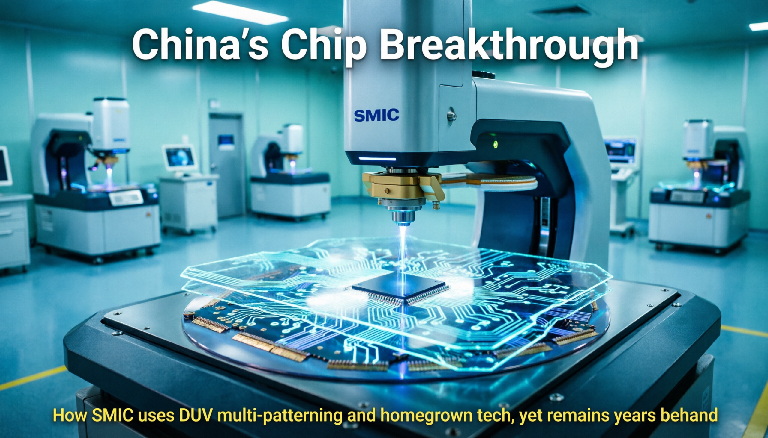
So China does something TSMC and Samsung did a decade ago as a temporary bridge — except for China, this is not a bridge. It is the destination. The technique is called multi-patterning, and SMIC’s most advanced variant is Self-Aligned Quadruple Patterning (SAQP).
How SAQP works, in simple terms:
- A pattern is exposed and etched onto the wafer.
- A “spacer” material is deposited around each feature.
- The original pattern is removed, leaving only the spacers.
- The spacers become the mask for the next etch.
- The process repeats, multiplying the pattern density four times over.
In effect, SMIC draws the circuit multiple times with slightly offset patterns, then combines them to produce features smaller than the light itself can resolve. It is slow, fragile, and expensive — but it is proven. TSMC and Intel both used multi-patterning to reach their earliest 7nm nodes before EUV was production-ready.
The American Enterprise Institute’s April 2026 report, The Lithography Loophole, documents this precisely: SMIC uses ASML immersion DUV scanners (the NXT:1980 series) with multi-patterning to produce near-frontier chips, legally purchased before DUV restrictions took full effect. Roughly 90 advanced immersion DUV machines were acquired by China in 2024 alone, valued at $5–7 billion and representing roughly a fifth to a quarter of the global installed base of that machine class.
3. What China Has Actually Produced
The proof is no longer theoretical. It is in consumer hardware that teardown labs have dissected:
| Chip | When identified | Process | Confirmed by |
|---|---|---|---|
| Kirin 9000S (Huawei Mate 60 Pro) | 2023 | SMIC 7nm-class (N+2), DUV + multi-patterning | TechInsights teardown |
| Kirin 9010 (Pura 70 series) | 2024 | SMIC 7nm-class (N+2), improved | TechInsights |
| Kirin 9030 (Mate 70 series generation) | 2026 | SMIC N+3 (5nm-class), still DUV | TechInsights (reported August 2026) |
The N+3 node is the critical data point. TechInsights confirmed the Kirin 9030 is manufactured on SMIC’s N+3 process — a 5nm-class node produced without EUV. Chinese research groups have been open about exploring whether DUV multi-patterning can reach 5nm, and 2026 appears to be the year that development started moving toward production.
None of this means the chips are cheap or abundant. Production is aimed at strategic customers — above all Huawei, which uses these fabs for both smartphones and AI accelerators (the Ascend line). The AEI report notes China targeted roughly 1.6 million high-end dies in 2026 for Huawei’s AI accelerators. That is real volume, but it is a fraction of what a TSMC-run fab of similar capacity would produce — and this is where the true cost of the workaround lives.
4. The Real Price of the Workaround
Multi-patterning does not violate physics. It defeats economics.
Every additional patterning pass multiplies the number of lithography, etch, deposition, and inspection steps on the hardest layers. Each step is a new opportunity for misalignment, contamination, or defects. The consequences are quantifiable:
- Lower yield. Industry estimates put SMIC’s 7nm-class yield in the 20–40% range (versus TSMC’s mature, high-yield EUV-based 7nm). For the 5nm-class process, analysts (including TD Cowen and Sam Wang’s Research) estimate yields below 20%, some as low as 15%.
- Higher cost per die. More steps, more masks (each mask costs tens of thousands of dollars), longer cycle times, and lower yield compound into a dramatically higher cost per usable chip.
- Lower throughput. Wafers spend far longer in the fab. The same machine capacity produces far fewer finished chips.
- Slower learning. Every yield improvement requires mastering a process that is exponentially more fragile than an EUV-based equivalent.
The math explains why no Western foundry would ever do this for a mainstream product. TSMC’s entire strategy is based on EUV single-patterning at the critical layers precisely because it is cheaper per good chip. For SMIC, the DUV route is not a choice — it is the only route available — and it is being paid for by state-backed strategic demand (Huawei, military, government AI) rather than by market economics.
5. 2026: China Starts Making Its Own Machines
The most significant development of 2026 is not SMIC’s yields. It is that China crossed a threshold everyone assumed was years away: domestic production of immersion DUV lithography machines.
In July 2026, The Information reported (and Reuters confirmed) that a Shanghai-based manufacturer had begun mass production of homegrown immersion DUV systems. The project draws on teams from several Chinese players — including Yuliangsheng (a startup affiliated with Huawei-backed equipment maker SiCarrier, whose immersion system SMIC has been testing since September 2025) and SMEE, the state-linked Shanghai Micro Electronics Equipment.
What matters about these machines:
- They are immersion DUV tools — the same class SMIC already uses for its advanced work.
- Through multi-patterning, they can in principle support 7nm-class (and potentially 5nm-class) production, though yields will trail imported machines.
- Most components are now domestic, though some critical parts still come from Japan.
- Volume is small: roughly 5 systems in 2026, ramping to about 20 in 2027, with early customers expected to include SMIC, Hua Hong, and CXMT.
The strategic significance is not that these machines are as good as ASML’s. They are not, and ASML’s Q2 2026 results (net sales of €9.3 billion, with the full-year forecast raised to €43–45 billion) show its lead is intact. The significance is that China now has a domestic alternative for the machines it depends on most — covering service contracts, spare parts, and future supply if Western export controls tighten further. It is an insurance policy against the next escalation.
6. The EUV Endgame: How Far Away Is China Really?
The DUV route gets China to 5nm-class chips at poor yields. It cannot plausibly take China to the 2nm–3nm frontier, because multi-patterning below ~5nm becomes catastrophically expensive even for a state-backed program. That is why the endgame is domestic EUV.
The balanced answer — based on The Diplomat‘s July 2026 analysis of the technical evidence — is that China is making real progress but remains years away. The gap can be decomposed into three technical moats:
| Moat | Status in China |
|---|---|
| Light source | Progress on generating 13.5nm light, but not yet at the power levels needed for commercially viable throughput. The ~250-watt power benchmark is the signpost to watch. |
| Precision optics | The hardest part. ASML depends on Zeiss mirrors polished to sub-nanometer precision (ion beam figuring). China’s best mirrors still require far more exposure time. |
| Photoresists | The least advanced area. EUV photoresists require parts-per-billion-to-trillion purity. For even ArF resists, less than 1% is domestically sourced. |
Estimates of when a domestic EUV machine becomes commercially usable range from a few years to decades. The more bullish observers (e.g., ASG’s Paul Triolo) suggest pilot-line capability around 2030, noting that some industry observers believe a Chinese EUV prototype has been functionally “complete” for some time. Skeptics counter that Chinese EUV progress often reflects reverse engineering and restricted-parts acquisition rather than independent innovation — and that catching up to where ASML is today means racing to where ASML will be tomorrow.
A note on sources: Chinese-language outlets periodically announce dramatic EUV “breakthroughs” (e.g., claims of 3nm trial production in August 2026, or a “Hyperion-2” EUV machine). Treat these announcements with strong skepticism. They are not corroborated by teardown evidence, independent testing, or Western industry analysts, and the pattern of past claims does not support them.
7. The Strategy Beyond the Machine
The lithography story, however, is only half of China’s strategy. The other half is engineering the system so that it does not need frontier chips in the first place:
- Advanced packaging. Chiplets, die stacking, and hybrid bonding let Chinese designers combine multiple 7nm dies into a package that behaves competitively with a single 5nm chip. This is the same direction the whole industry is moving — China is simply forced to lean on it harder.
- Software and algorithmic efficiency. The sanctions workaround that produced DeepSeek, Qwen, and other open-weight models shows a pattern: when China cannot match Western hardware, it compensates with algorithmic cleverness that squeezes more performance from fewer FLOPs.
- Turning scarcity into a moat. As we analyzed in our look at how China is turning resource scarcity into a competitive advantage, the constraint is forcing China to optimize for efficiency in ways that may ultimately be exportable advantages.
- AI workloads that tolerate lower efficiency. Inference workloads — which dominate much of AI deployment — are more forgiving of slightly larger, less efficient silicon than cutting-edge training runs. A 7nm Ascend accelerator is “good enough” for a large fraction of China’s domestic AI demand.
The deeper point is that China’s chip strategy is not trying to win the same race as TSMC. It is trying to become self-sufficient enough to be unsanctionable, even if it never becomes the world’s best. As semiconductor analyst Dan Hutcheson put it, the harder China runs, the more it may stay in place relative to the frontier — but being stuck two generations behind is still a very different outcome than being cut off entirely.
8. How Far Behind Is China, Really?
| Metric | TSMC (frontier) | SMIC (best available) |
|---|---|---|
| Latest logic node | 3nm–2nm in production (EUV) | 7nm in production; 5nm-class (N+3) ramping, low yield |
| Lithography | EUV + DUV | DUV multi-patterning only |
| Yield at advanced node | High | Estimated 20–40% (7nm); below 20% (5nm-class) |
| Generation gap vs. NVIDIA silicon | H100 on N4, B200 on N3P | ~3–4 generations behind |
| Primary driver | Market economics | State-backed strategic demand |
For context: NVIDIA’s H100 is built on TSMC’s 4nm-class node; the B200 on 3nm-class. SMIC’s best available process sits roughly three to four generations behind the silicon powering Western AI. That gap is exactly why the AI chip competition between Chinese and Western suppliers remains so asymmetric — and why every Chinese AI advance gets scrutinized for how it was achieved within the equipment constraints.
9. What Happens Next
The most important variables to watch are not technical — they are regulatory and economic:
- The MATCH Act. As of April 2026, this U.S. legislative proposal would impose countrywide restrictions on ASML DUV immersion lithography in China — a fundamentally different escalation from entity-based controls. It would also bar servicing of existing machines, threatening the ~90-machine fleet China currently depends on. This is the single biggest risk to China’s current strategy.
- Domestic DUV ramp. Whether the ~5 (2026) and ~20 (2027) homegrown immersion machines actually work at production scale in SMIC, Hua Hong, and CXMT fabs. If they do, China’s equipment supply chain becomes meaningfully insulated. If they fail in the field, the program needs several more generations.
- N+3 yields. Whether SMIC’s 5nm-class process climbs from below-20% yields toward something economically sustainable. This determines whether the Ascend/Kirin roadmap can scale.
- EUV light source power. Whether China reaches the ~250W benchmark on a domestic EUV light source — the signpost that separates lab demos from manufacturing viability.
FAQ
How does China make 7nm chips without EUV?
By using older 193nm DUV immersion lithography with a technique called multi-patterning (specifically SAQP), which exposes each chip layer multiple times with offset patterns to achieve features smaller than the light wavelength can resolve.
Why doesn’t China just buy EUV machines?
Export controls — enforced by the Netherlands and the U.S. since the late 2010s — bar the sale of EUV machines to China. ASML is the only manufacturer in the world.
Does this mean China has matched TSMC?
No. SMIC’s 7nm process works, but yields are estimated at 20–40% (versus TSMC’s high-yield EUV-based process), cost per chip is far higher, and the 5nm-class process is still ramping at below-20% yields. China is roughly three to four generations behind the frontier.
How many DUV machines does China have?
Roughly 90 advanced immersion DUV machines were acquired in 2024 (worth $5–7 billion), representing roughly 20–25% of the global installed base of that class — all legally purchased before DUV restrictions fully tightened.
Has China built its own lithography machines?
Yes, for DUV. In July 2026, China began mass production of homegrown immersion DUV machines, with roughly 5 units expected in 2026 and ~20 in 2027, destined for SMIC, Hua Hong, and CXMT. Domestic EUV is years away.
When will China have its own EUV machine?
Estimates range from a few years to decades. The most bullish credible scenario points to pilot-line capability around 2030. The three hard bottlenecks are the light source power, Zeiss-class precision optics, and EUV photoresists.
Why is this a problem for the U.S. even if China stays behind?
Because China doesn’t need to win the technology race — it needs to become unsanctionable. A self-sufficient DUV-based industry, advanced packaging, and algorithmic efficiency give China chips “good enough” for domestic AI and defense demand, regardless of how far behind the frontier it remains.
Key Takeaways
- China produces advanced (7nm, and now 5nm-class) chips without EUV by using DUV immersion multi-patterning — a technique that works but costs heavily in yield, throughput, and price per die.
- The technique is proven in commercial hardware: SMIC’s N+2 (7nm) and N+3 (5nm-class) processes are confirmed in Huawei’s Kirin chips by TechInsights.
- In July 2026, China began manufacturing homegrown immersion DUV machines — a strategic insurance policy against further export controls, still at small scale (~5 units in 2026).
- Domestic EUV remains years away, bottlenecked by light-source power, precision optics, and photoresists. Chinese “breakthrough” claims should be treated with skepticism.
- The real risk to the U.S. strategy is not that China reaches the frontier — it is that China becomes self-sufficient enough to be immune to sanctions, using advanced packaging, AI inference tolerance, and software efficiency to make “good enough” chips.
- Watch: the MATCH Act, domestic DUV field performance, N+3 yields, and the EUV light-source power benchmark.
Conclusion
The answer to “how does China make advanced chips without the most complex machine on Earth” is: it doesn’t avoid the complexity — it relocates it. Instead of one incredibly complex EUV machine printing a layer in a single pass, China runs far more exposures through older, available machines, absorbing the cost in yield, time, and money. The chips exist, they ship in commercial products, and their existence has already reshaped the U.S.–China technology war.
But the gap never closed. China trades efficiency for availability, and that trade has a hard floor: DUV multi-patterning can reach 5nm-class silicon at punishing cost, but it will not reach the 2nm frontier where the industry is heading. The race China is actually running is not for first place. It is for the ability to keep running at all — and in 2026, with domestic DUV machines entering production, it is closer to that goal than it has ever been.
Note: Yield and production figures are industry estimates from teardown analyses, analyst reports (TD Cowen, Sam Wang’s Research, TechInsights), and the AEI report “The Lithography Loophole” (April 2026). Chinese-language claims of EUV breakthroughs are not independently corroborated and should be treated as unverified.

Independent technology writer focused on artificial intelligence, emerging technologies, and digital innovation. Covers AI applications in sports, productivity, and online business.